🎉I have already sent to manufacture the final version of LibreServo to JLCPCB!🎉
In total there have been 50 PCB boards (50 because they were the same price as 30) of 0.8mm thick and of the highest possible quality; 6 layers, ENIG finish, epoxy filled and capped vias, PCB material upgraded to FR-4 TG155... Everything came out to me for about $93.24, which with VAT and shipping goes up to $118.18. That gives a base price of about $2.36 per LibreServo. Making the four-layer version of LibreServo, in HASL finish (with lead), FR-4 TG135-140 material and tracks simply covered with solder mask comes out to $56.20, which with VAT and shipping goes up to $75 for a total of $1.5 each LibreServo. Personally I think that making it in 6 layers and the rest of the improvements are well worth 0.86$ per board, but it is something that each one will have to value and that certainly LibreServo is going to work equally well in both configurations.
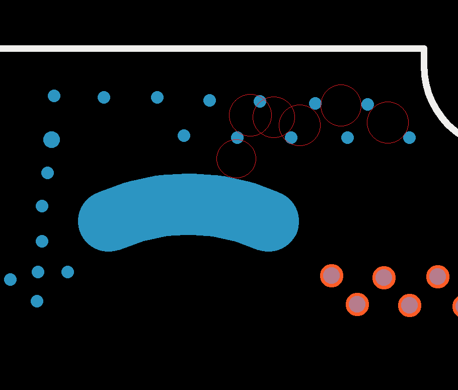
However, it seems that every step I take on LibreServo I always encounter some problem and this time was not going to be the exception. For one hand, JLCPCB have changed their pricing policy. Since "always" in 4-layer boards or more, the vias that were included in the price were 0.2 mm and higher, but a few days ago they have changed it and now they differentiate between vias up to 0.3, 0.25, 0.20 and 0.15 mm. By default I always make 0.3 mm vias, but in LibreServo I had 7 vias at 0.25 mm that I had put in places with very tight space. These vias and the adjacent tracks I have been forced to modify accordingly so that the price of LibreServo does not go up.
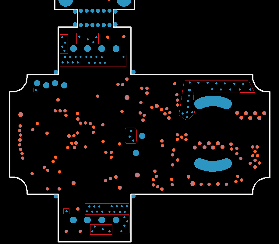
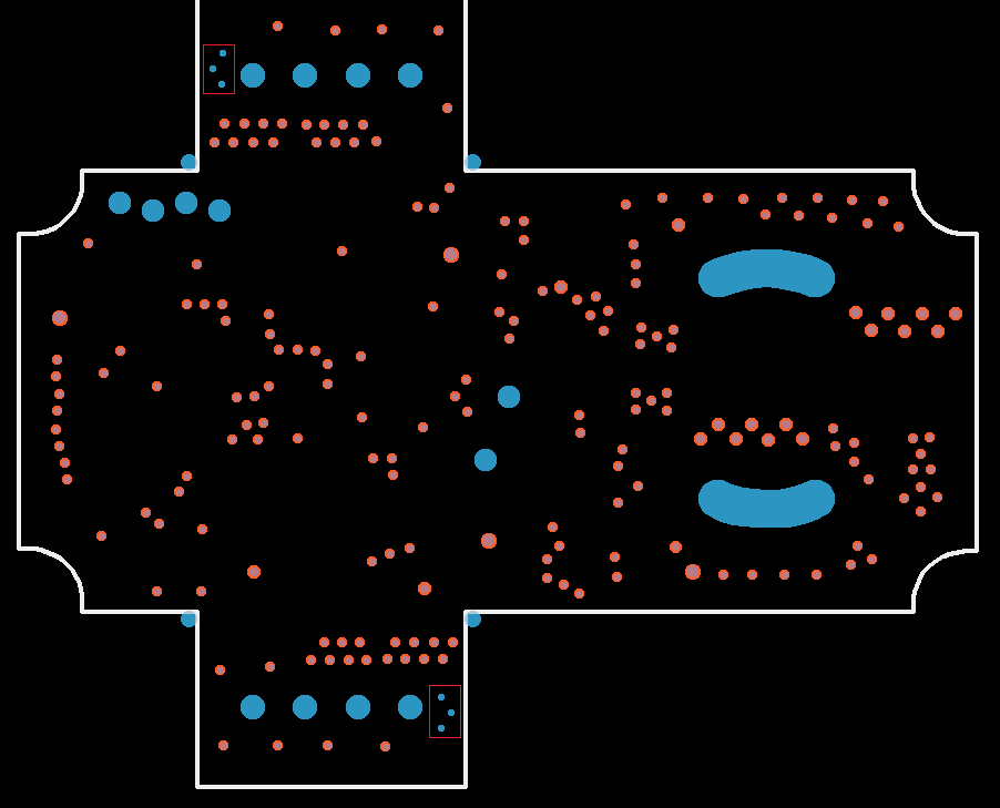
On the other hand, I told you previously that I had had a small problem with the vias, which in JLCPCB's 6-layer service come filled with epoxy and covered in copper (a great improvement), but quite a few of them came unfilled. At the time I thought it was a defect of JLCPCB because I did not see any relationship between copper coated and non copper coated vias... Well, there was. As I didn't believe that the error was JLCPCB's, I decided in this last order to put the option to let me check the manufacturing files before they made it. And thank goodness I did! Sure enough, again a lot of vias were uncovered in copper. After complaining to JLCPCB they told me the real reason. The vias that you want to be filled with epoxy and covered in copper have to be more than 1 mm from any other holes and/or vias that are tinned but not covered in copper. That is. If a via is next to a normal hole that is not tinned and you only have it for mounting (for example), there is no problem, but if a via is within 1 mm of the holes of a trhough-hole type capacitor, or a JST connector, then that via cannot be filled with epoxy... and now, any via that is within 1 mm of this via that cannot be filled with epoxy, cannot be filled with epoxy either... and so on and so on in a chain. Hence, vias in completely distant positions were unfilled, because there was a chain of vias that were within 1 mm of each other that could not be filled with epoxy. Finally I changed the position of most of the vias and only left unfilled three vias next to the JST connectors because there was no physical space to move them. In the following pictures everything is clearer, in orange are the epoxy filled vias and in blue are vias that will not be filled with epoxy. It should be noted that filling the vias with epoxy and covering them does not change the operation of LibreServo in any way, in my case it is mostly aesthetic as it allows printing on covered vias, although it is also true that it facilitates soldering components when you have vias on the pads, which in LibreServo for space problems is something that exists, although exceptionally.
Errors and fixes
After several emails, always very cordial, the final version of LibreServo (the hardware) is in production.


