Generally the final production of a PCB is exactly the same as the gerber files we have generated, but there are times when there is a doubt if the production is going to be exactly the same as we want, for example if we have a tinned slot, or if we have epoxy filled vias and we want to make sure we meet the specifications as we saw in the article on last minute changes in LibreServo. In all these not so usual cases, in JLCPCB we have the option to check the production files before our PCB goes into production. Be careful! we will only have 24 hours to confirm the production files, otherwise they will autoconfirm, so don't lazy.
Confirm production file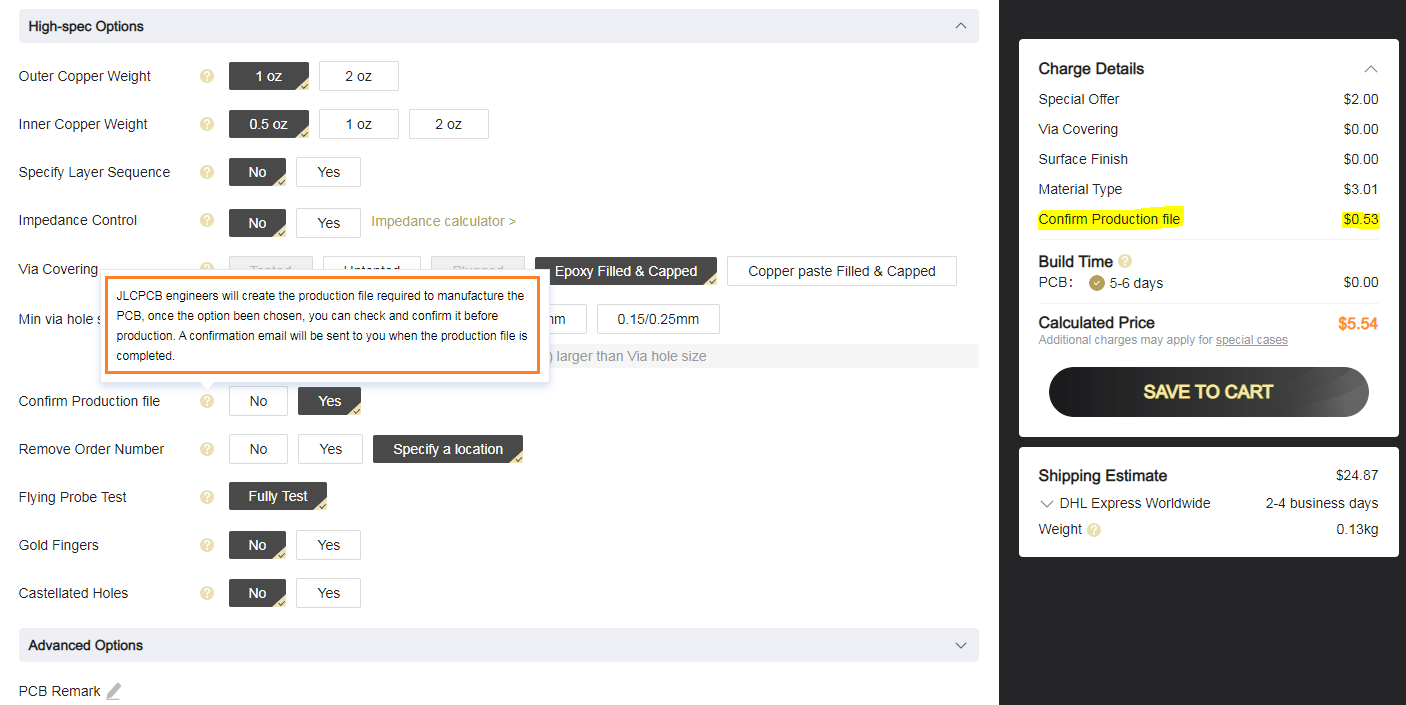
Once you have selected the option when placing your order, generally within a few hours they will have the production files ready for you to review. You will receive an email notification, but it is worth checking the website from time to time in case the email does not arrive. In your "Order History" you will see a button to confirm the production files, click on this button and you will be able to download the production files. In the following image I have already confirmed the production files, but the screen is exactly the same except that instead of putting that the files are already confirmed, a selection appears to confirm or reject the production files.
Download Production file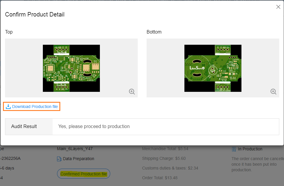
Once the production files are downloaded, they are a compressed .rar file, inside you will find three folders:
- info which contains internal production information (we are not interested in this)
- ok which is where the production files are located
- yg which is where the gerber files that we have uploaded are located
In the case of epoxy filled vias, the layer we are interested in is sk, where are the vias that will be filled with epoxy and capped with copper and the drl layer, where are all the holes that will be made in the PCB. The rest of the layers are all pretty self-explanatory. In the following image you can see in blue all the holes and slots that will be made, and in orange, all the vias that will be filled with epoxy. If you look, there are three vias on each side that will not be filled with epoxy. The reason for this is explained in the previous article.
Ucamco gerber viewer. Detail of epoxy-filled vias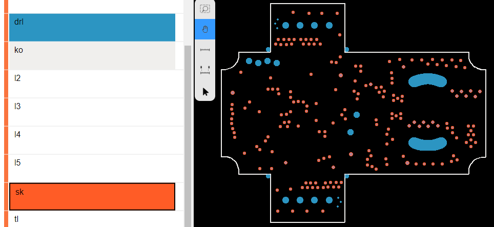
From now on, if we have any doubt that our gerbers are going to be produced exactly as we want, we know how to check.